X Ray Imaging With a Silicon Microstrip Detector
Tadej
Mali 1, 2, Vladimir Cindro 1
and Marko Mikuž 1, 2
1 Jožef
Stefan Institute, Jamova 39, Ljubljana
2 Department
of Physics,University of Ljubljana,
Jadranska 19, Ljubljana
Abstract
A small (3 mm wide) scanning test system was built
and tested, using silicon microstrip detectors. Strips are oriented in
parallel with the incident photon beam. High efficiency obtained in this
way, depends mostly on the size of the guard ring. Images of simple objects
were taken, contrast, detection limit and position resolution were studied.
1. Introduction
Breast cancer is a disease, which affects one out
of 13 women in their life and one out of 25 dies because of it [1].
In order to cure the cancer effectively, an early and reliable diagnosis
is essential. Therefore it is advisable for women over 50 years old to
take regular X-ray examinations (mammography). However, exposure to X-ray
radiation can provoke the disease itself. Therefore, it is necessary to
minimize the delivered dose per mammographic examination. This can be achieved
by using efficient, high resolution detectors for X-ray photons. One of
the possibilities are. silicon microstrip detectors, which can have an
efficiency in excess of 50%.
2. Imaging
2. 1 Photon detection
In order to make a high contrast image, soft x-rays
are used. Their energy ranges, depending on the tissue thickness, from
17 (2 cm of tissue) to 23 keV (8 cm of tissue) [2].
The mean free path of X-rays
in silicon is between 0.60 mm (17 keV) and 1.6 mm (23 keV) [3],
therefore the absorbing depth in the detector should be a few millimeters
in order to efficiently absorb the incident photons.
A silicon microstrip detector is an array of
thin, parallel, reverse biased p-n diodes. A traversing ionizing particle
or photon generates electron-hole pairs in the depleted area. The generated
charge is then collected and read out. The signal is directly proportional
to the energy of incident photons and the average energy required to generate
an electron-hole pair is 3.6 eV. Microstrip detectors are usually produced
on thin (0.3 mm) silicon wafers and the length of strips is usually a few
centimeters. If we orient the detector in such a way, that the incident
photons hit the detector from the side (fig.
1), it acts as a pixel detector, where the size of the pixel is determined
by the thickness of the wafer and the strip pitch. A 2D image can be obtained
by scanning the object in the direction perpendicular to the detector plane.
The main source of noise in silicon microstrip
detectors is the leakage current, which is caused by impurities or imperfections
of the crystal lattice. Cutting the detector out of the wafer damages the
crystal structure at the edges. This results in an increase of the leakage
current [4].
Therefore the strips on the detector have to be kept away from the edge
and a guard ring structure is inserted between strips and the edge of the
detector. This represents a dead region of the detector, because the photons
absorbed in the guard ring can not be detected. The maximum efficiency
of the detector is thus determined by the distance between the edge and
the strips. For example, a detector with 0.30 mm wide guard ring and 22
keV incident photons, has an efficiency of about 80%.
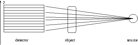 Figure 1: Imaging
with silicon microstrip detectors.
Figure 1: Imaging
with silicon microstrip detectors.
2. 2 Readout Electronics
X-ray imaging with silicon microstrip detectors is
a single photon detection technique. Therefore an electronic system is
required, which is capable of standalone multichannel, real-time, high-rate
counting of current pulses, resulting from the hits of the photons on the
pixels in the detector.
We have used a mixed analog-digital integrated
circuit CASTOR (Counting
and Amplifying SysTem fOr Radiation detection) [5,
6, 7], developed by LEPSI, Strassbourg..
It is made in 1.2 m VLSI technique [5]
and optimised for the use in the Syrmep experiment [8].
Each channel consists of an analog part (charge sensitive preamplifier,
shaper, filter) which is connected to a digital part (16-bit counter) via
a comparator (only pulses, higher than the user-defined threshold, are
counted); see fig.
2. The counting rate capability is limited by the analog part and it
is about 100 kHz. After the acquisition the counters are connected into
a shift register, the contents are read out and the IC is ready for the
next acquisition.
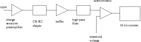 Figure 2: CASTOR block
scheme.
Figure 2: CASTOR block
scheme.
We have measured the performance of the CASTOR
circuit (gain, noise, counting rate) before mounting it to the detector.
In order to measure the gain (G) of the analog
part, a series of voltage steps () was applied to the capacitor (capacitance
Ci) coupled to the input of preamplifier The number of detected pulses
as a function of the threshold voltage. was measured and a counting curve
obtained (fig.
3a). The response of the circuit is the threshold voltage, where half
of the input pulses are counted. Using a capacitor, the calibration curve
for the analog part of the circuit was obtained (fig.
3b). It can be seen, that the response is linear for the input charge
up to 2.5 fC (corresponding to approx. 55 keV photon). The gain (in the
linear region) was determined to be 234 (2) (12) mV/fC, where the first
error is statistical and the second systematic. The gain of different channels
is the same within 10%, and it slightly decreases with the input capacity
(Ci): G=(234 (2) -(6.7 (5))xCi/pF)
mV/fC. The errors are statistical, while the systematic errors are given
by the error of the gain.
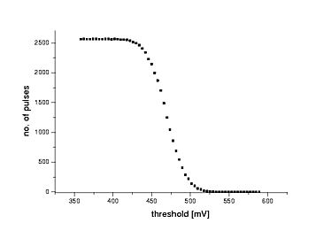 a) counting curve
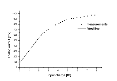 b) The calibration curve of the analog part
Figure 3: Calibration
of the analog part.
b) The calibration curve of the analog part
Figure 3: Calibration
of the analog part.
The noise was measured with the input capacitor
grounded. Noise was determined by the standard deviation of a gaussian,
which was fit on the derivative of the counting curve. Knowing the gain,
the noise of the circuit can be expressed in ENC units. We found
the noise to be: ENC=76 (4) (8) e0
+ 6.8 (0.7) (0.7)e0/Ci;
Ci is the stray capacitance at the input; the first error
is statistical and the second systematic.
2. 3 Detector
A silicon microstrip detector, which was made as
a test structure for the development of the DELPHI spectrometer [9]
at CERN was used. The detector was 0.3 mm thick with a strip pitch of 0.1
mm. Two neighbouring strips were bonded together, resulting in the pixel
dimensions of 0.2x0.3 mm2. The length of
the strips was about 2 cm. The detector was cut 0.6 mm from the edge, giving
an efficiency of 65% for 22.5 keV photons. The capacitance of a strip towards
its neighbourhood was estimated to app. 3 pF.
The response of the detector connected to the
readout electronics was tested, using a variable X-ray source. By changing
the threshold voltage, the source spectrum was scanned. Since the energy
of the photons is known, it was possible to determine the relation between
the energy (E) of incident photons and the output of the analog part (Vout).
The relation between Vout and E
is: Vout=-75 (3) (4) mV + 9.5 (0.2)
(0.5) mV/E; the first error is statistical and the second systematic.
2. 4 Imaging System
The imaging system is shown on fig. 4. The detector
and CASTOR are glued
to a PCB, where the bias and control currents and voltages are filtered.
The PCB is shielded by a metal box.
The control card consists of an analog and a
digital part. The digital part is an interface between the computer and
the IC; there is a level translator and a decoder, which accepts the controls
from the PC and generates the control signals for CASTOR.
In the analog part of the control card there are biasing for the IC and
control current/voltage sources for its analog part. There resides also
a filtering system for the detector biasing.
The object under inspection was scanned using
a moving stage. The stage can move the object in minimal steps of 0.0125
mm.
The source of X-rays was an X-ray tube with a
tungsten anode, operating at 25 kV anode voltage.
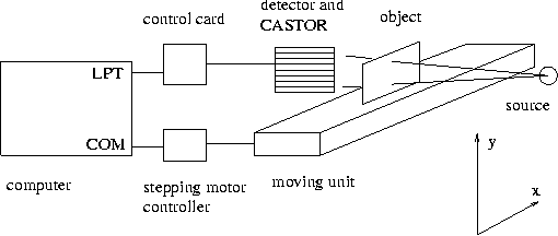 Figure 4: Imaging
system.
Figure 4: Imaging
system.
2. 5 Images and Analysis
In X-ray imaging it is essential to distinguish small
objects embedded in a tissue. This is possible because of different attenuation
properties of the inspected tissues. We define the contrast (C) as [2]:
 (1)
where N1 is the number of photons per pixel in the
area, with tissue only (background), while N2 is the number of photons
per pixel in the area, where they pass the object. The signal (S), that
we are interested in, is the difference between detected photons in the
background and in the area, where the object resides:
(1)
where N1 is the number of photons per pixel in the
area, with tissue only (background), while N2 is the number of photons
per pixel in the area, where they pass the object. The signal (S), that
we are interested in, is the difference between detected photons in the
background and in the area, where the object resides:
 .
(2)
Because of fluctuations in the background (noise),
the signal must be significantly higher than the noise. The working condition
for the signal to noise ratio (SNR) requires it to be above 5 to clearly
see the object. As the noise increases as, SNR increases as:
.
(2)
Because of fluctuations in the background (noise),
the signal must be significantly higher than the noise. The working condition
for the signal to noise ratio (SNR) requires it to be above 5 to clearly
see the object. As the noise increases as, SNR increases as:
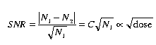 (3)
Therefore, objects cannot be seen until the delivered
dose is high enough for the SNR to be above 5.
(3)
Therefore, objects cannot be seen until the delivered
dose is high enough for the SNR to be above 5.
The described system was used to make images
of simple objects - a thin (0.1 mm) Al foil, with small holes through it
(fig.
5). The object contrast is approx. 0.07 and it corresponds to a microcalcification
with a diameter of 0.05 mm in woman's breast. The diameters of the holes
are: (upper row, from left to right) (two holes, which cannot be distinguished
and appear as a single one), 0.40, 0.50, 0.58, 0.65, 0.80 and 0.90 mm.
There is also a hole in the lower left corner; its diameter is 0.25 mm.
The effect of increasing the dose can be seen
in fig.
5. The noise of the background was calculated as the rms of the number
of detected photons in the vicinity of the holes and the signal was calculated
as the difference between the number of detected photons in the background
and the number the maximum number of photon counts in a pixel in the signal
region.
The image contrast was calculated as a relative
difference between signal and background (eq.
1) and the values obtained ranged between 0.06 (0.80 mm hole) and 0.01
(0.25 mm hole), depending on the size of the object.. The contrast is in
good agreement with that expected for big objects and is lower for objects
comparable or smaller than the pixel size. This can be explained by signal
sharing between the neighbouring pixels.
The obtained SNR was plotted and fitted by a
square root function (fig.
6). Considering the requirement SNR=5, the required dose per
investigation could be calculated [10].
The results are summarised in table 1. Low contrast objects require higher
dose, as predicted in eq.
3.
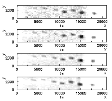 Figure 5: Images of a simple
object, taken at different exposure times (1, 2, 5 and 9s). The exposure
time of 1 s equals approx. 40000 detected photons per pixel in the background.
The measured contrast in the picture is between 0.01 and 0.06.
Figure 5: Images of a simple
object, taken at different exposure times (1, 2, 5 and 9s). The exposure
time of 1 s equals approx. 40000 detected photons per pixel in the background.
The measured contrast in the picture is between 0.01 and 0.06.
tissue thickness
[cm] |
photon energy
[keV] |
2r=0.5 mm
dose [mGy] |
2r=0.25 mm
dose [mGy] |
| 2 |
17 |
1.2/h |
8/h |
| 4 |
20 |
1.8/h |
13/h |
| 6 |
22.5 |
2.0/h |
14/h |
| 8 |
23 |
5.4/h |
39/h |
Table 1: Estimation of the superficial dose per
investigation, required to see an object with the given diameter and contrast
of 0.07 (h is the efficiency of the detector).
3. Conclusions
The first tests of the system were successful. The
performance of the readout electronics is in good agreement with manufacturer's
specifications.
The measurements with a thin Al foil (0.1 mm)
showed, that low contrast objects (C=0.07) with a diameter of 0.5 mm, embedded
in 4 cm thick tissue could be seen with a superficial dose of 2.8 mGy per
investigation, using a detector with 65% efficiency. Further improvements
in spatial resolution and image processing would significantly improve
the detectability of objects. Together with higher efficiency of the detector
(reduced dead region) this would also contribute to a lower superficial
dose.
To obtain an objective comparison between the
conventional method (film) and the new technique (silicon microstrip detectors),
a test of our system with a conventional mammographic phantom is planned.
 Figure 6: SNR as a
function of number of detected photons in the background.
Figure 6: SNR as a
function of number of detected photons in the background.
4. References
[1] G. Stafford, Mammography
Basic Principles, American Medical Association, Chicago, 1992
[2] W. Swindell,
S. Webb, The Physics of Medical Imaging, IOP Bristol and Philadelphia,
1992
[3] Mucal on The Web,
http://www.csri.iit.edu/mucal.html
[4] F. Arfelli et.
al., Developments in the field of silicon detectors for digital radiology,
, Nuclear Instruments and Methods A377, 1996, 508-513
[5] G. Comes et. al.
CASTOR a VLSI CMOS Mixed Analog-Digital Circuit for Low Noise Multichannel
Counting Applications, Nuclear Instruments and Methods A377, 1996, 440-445
[6] CASTOR 0.0, User Manual, 1995
[7] CASTOR 1.0, User Manual, 1996
[8] F. Arfelli et. al.,
Silicon Detectors for Synchrotron Radiation Digital Mammography, Nuclear
Instruments and Methods A353, 1994, 366-370
[9] V. Cindro et.
al., The design of silicon ministrip detectors for the DELPHI Very Forward
Tracker, Nuclear Physics B44, 1995, 292-295
[10] T. Mali, Postavitev
sistema za rentgensko slikanje s silicijevimi mikropasovnimi detektorji,
Diplomsko delo, Oddelek za fiziko, Univerza v Ljubljani, 1997.