Silicon and diamond detectors
Most of the work on silicon detector development was performed in the framework of ATLAS and CERN-RD50 collaborations. Our group is also active in the development of diamond tracking detectors in the framework of the RD42 collaboration.
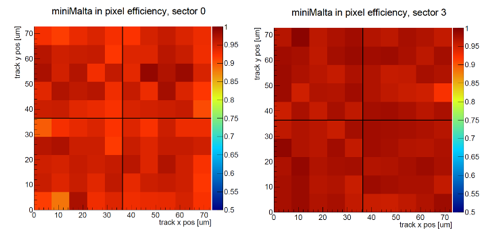
Work on upgrade of ATLAS detector for the HL-LHC was the main activity in the development of silicon detectors. This includes measurements of silicon strip detectors for ITk and development of LGAD for HGTD as described above. In addition to work for ATLAS extensive measurements with depleted CMOS detectors were made in 2020. Studies were done with test structures on prototype chip RD50-MPW2 developed by the RD50 collaboration. Depleted CMOS is suitable technology for monolithic tracking detectors for high radiation environments (figure 6) as well as for applications where amount of material in tracking volume must be minimized. Depleted CMOS ensures also fast charge collection [15] enabling good time resolution which is becoming increasingly important in all types of applications.
Large number of measurements of space charge concentration as a function of irradiation fluence were made using E-TCT method [16]. Removal of initial acceptors (boron) caused by neutron irradiation was studied for p-type substrates with different initial resistivities. A study of behaviour of effective space charge concentration and detector current as a function of annealing time at 60° C was made. A system for E-TCT measurements with active CMOS pixels on RD50-MPW2 chip was built.
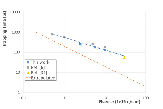
Our group is working on development of detectors for next generation of hadron colliders e.g. (Future Circular Collider - FCC). Work includes measurements of detector response after irradiation to extreme hadron fluences of 1017 n/cm2 and beyond. In 2020 extensive charge collection measurements with thin planar detectors were made and results published in [17] (figure 8).
Members of F9 department continued work on diamond detectors for charged particles. Studies of effects of irradiation with protons and neutrons were made with poly and monocrystalline artificial diamonds [18]. In the year 2020 measurements of transients caused by two(and more) photon absorption enabling three-dimensional mapping of detector response.
As a part of the bilateral project with NürDAM institute, Bolu, Turkey the MOS-FET dosimetry sensors were designed, tested and shown to be appropriate for the use in ATLAS experiment [19].
[15] M. Dyndal et al., “Mini MALTA : radiation hard pixel designs for small-electrode monolithic CMOS sensors for the High Luminosity LHC”, 2020 JINST 15 P02005.
[16] R. Klanner et al., “Determination of the electric field in highly-irradiated silicon sensors using edge-TCT measurements”. Nucl. Instr. & Meth. A 951 (2020) 162987.
[17] I. Mandić et al., “Measurements with silicon detectors at extreme neutron fluences”, 2020 JINST 15 P11018.
[18] L. Bäni et al. (RD42 collaboration), ”A study of the radiation tolerance of CVD diamond to 70 MeV protons, fast neutrons and 200 MeV pions.” Sensors, Vol 20, 6648 (2020).
[19] G. Kramberger et al, “Development of MOS-FET dosimeters for use in high radiation fields”, Nucl. Instr. & Meth. A 978 (2020) 164283.